PCB for AI Accelerators
World Class Top Company ISU PETASYS
Overview
PCBs for AI Accelerators Equipped with AI Engines
AI accelerators are specialized processors designed to handle large-scale AI computations—such as matrix operations and deep learning—more quickly and efficiently than CPUs and GPUs. They are a core component of AI servers, improving AI training and inference performance as well as overall power efficiency. Leveraging its advanced high‑layer PCB technology, ISU Petasys has entered the AI accelerator PCB market to secure new growth drivers and is continuing to focus on technological innovation and product development. The technology and expertise accumulated through this new business are expected to create synergies when applied to our existing networking business.
Product
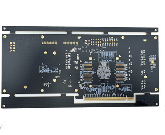
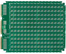
Probe Card connects semiconductor chips with test equipment. The probe pin mounted on the Probe Card contacts on a wafer to be used for sorting defective semiconductor chips.
Product Image
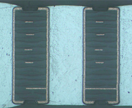
Layer Structure
Specification
| Item | Specification |
|---|---|
| Thickness | 2.5mm |
| PCB Size | 480×480mm |
| DHS(Min) | Φ0.2 |
| Layer Count | 18L |
| Surface Finish | ENIG + HARD GOLD |
It is one of the boards included in semiconductor test equipment together with the Probe Card. It is used for the purpose of an interface between tester and semiconductor.
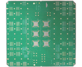
Product Image
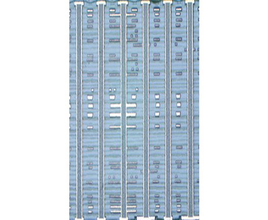
Layer Structure
Specification
| Item | Specification |
|---|---|
| Thickness | 5.0mm |
| PCB Size | 403x403mm |
| DHS(Min) | Φ0.125 |
| Layer Count | 52L |
| Surface Finish | ENIG |
It is a board for the purpose of an interface used for Burn-In Test, which performs the role of transmitting various signals transmitted from the burn-in system to semiconductors. It is used for sorting early defects by giving bad conditions such as high temperature or high pressure to implement a resistance test and for evaluating product characteristics.
Product Image
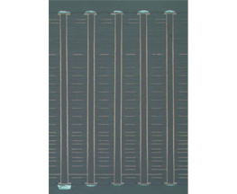
Layer Structure
Specification
| Item | Specification |
|---|---|
| Thickness | 1.6mm |
| PCB Size | 450×571mm |
| DHS(Min) | Φ0.35 |
| Layer Count | 8L |
| Surface Finish | Hard Gold + ENIG |
| Special | Polyimide Material |
Product Introduction Video

Seoul Office : 84, Sapyeong-daero, Seocho-gu, Seoul, Korea (06575) TEL : +82-2-590-5100 FAX : +82-02-590-5108
COPYRIGHT ISU PETASYS. ALL RIGHTS RESERVED.